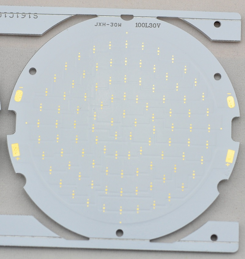
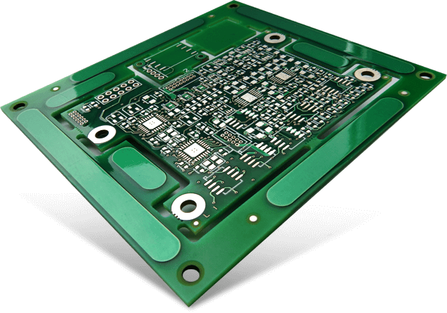
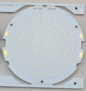
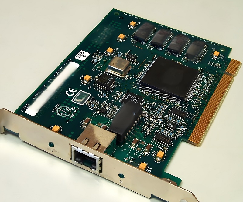
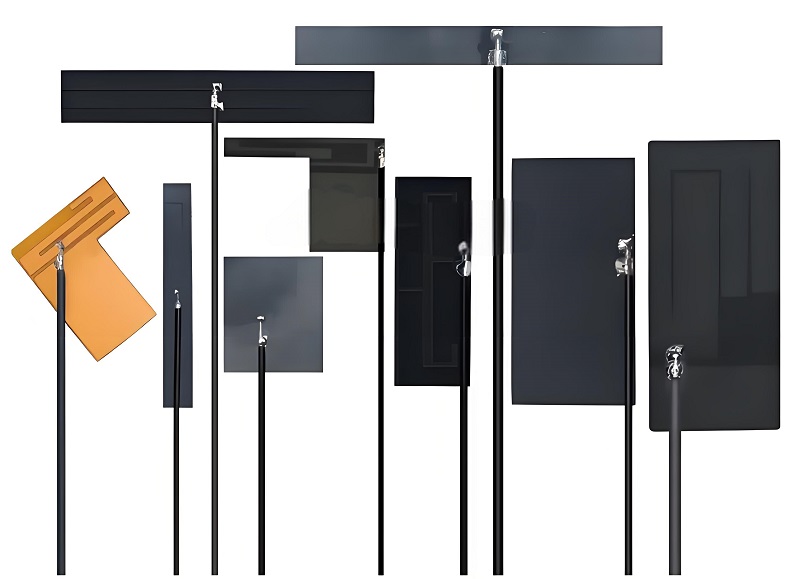
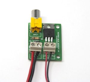
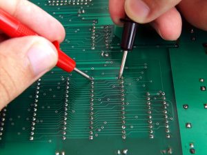
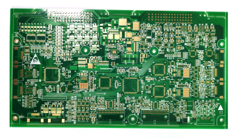
Metal core PCB is designed for applications requiring efficient heat dissipation, making it ideal for high-power electronics. Unlike standard PCBs, it features a metal base, typically aluminum or copper, that enhances thermal conductivity and improves durability. This design helps prevent overheating, ensuring stable performance in LED lighting, automotive systems, and power electronics. As industries demand reliable and heat-resistant circuit boards, metal core PCBs have become a preferred choice.
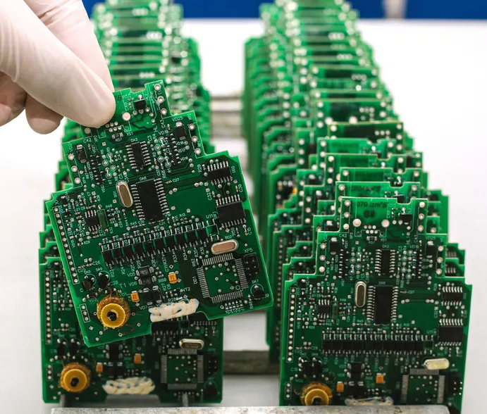
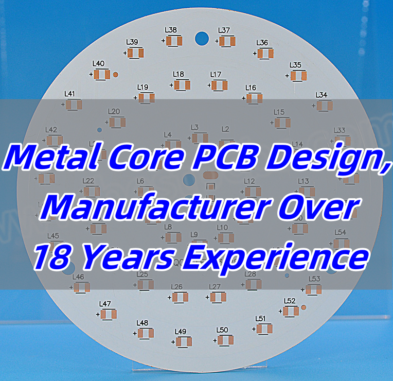
Best Technology has over 18 years of experience designing metal core PCBs. We are a professional metal core PCB manufacturer, mainly involved in all types of PCB manufacturing. If you need a metal core PCB, please feel free to contact us at sales@bestpcbs.com.
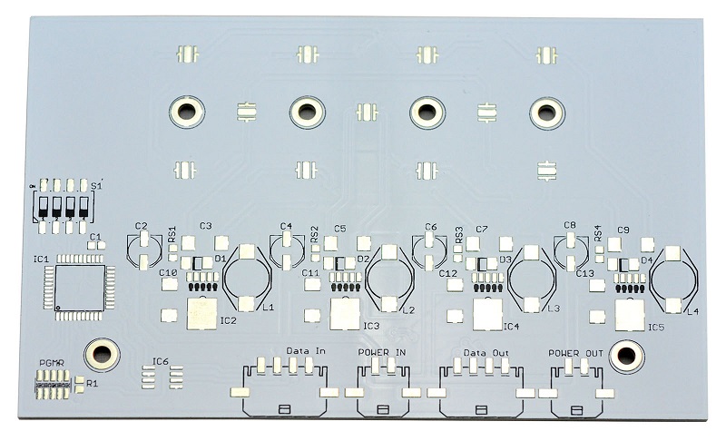
What is a Metal Core PCB?
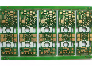
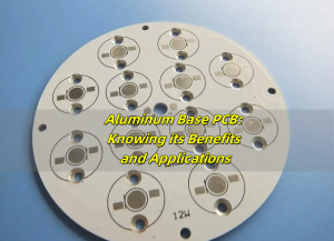
A metal core PCB (MCPCB) is a specialized type of printed circuit board that features a metal core instead of the standard FR4 or other non-metallic substrates. The metal core, typically made of aluminum, copper, or steel, helps dissipate heat efficiently, making it a preferred choice for high-power applications such as LED lighting, automotive electronics, and power conversion systems.
Unlike regular PCBs, which rely on thermal vias or external heat sinks for cooling, MCPCBs conduct heat directly through their metal base. This results in better thermal management, increased reliability, and a longer lifespan for electronic components. If you’ve ever wondered why some circuit boards perform better under high temperatures, chances are they are using metal core PCB technology.
What Are the Different Types of Metal Core PCBs?
Metal Core PCBs (MCPCBs) are classified based on three key dimensions: Layer Structure, Heat Dissipation, Application-Specific Features.
1. Classification by Layer Structure
Single-Layer MCPCB
- Structure: A metal base, an insulating dielectric layer, and a single copper layer for circuit traces.
- Best For: LED lighting, power supplies, and basic thermal management applications.
- Key Benefit: Simple and cost-effective with efficient heat dissipation.
Two-Layer MCPCB
- Structure: Two copper layers put on the one side of MCPCB, with an aluminum or copper base.
- Best For: Power circuits requiring more routing flexibility than single-layer MCPCBs.
- Key Benefit: Improved circuit complexity and higher current capacity.
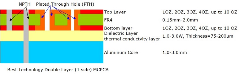
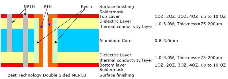
Double-Sided MCPCB
- Structure: Copper layers on both sides of the metal core, connected via plated through-holes (PTHs).
- Best For: Automotive control systems, industrial power converters, and motor drivers.
- Key Benefit: Enhanced circuit routing options and improved electrical performance.
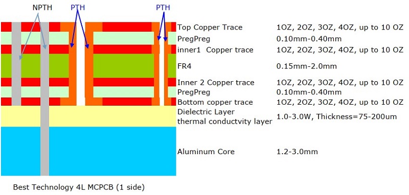
Multilayer MCPCB
- Structure: Multiple copper and dielectric layers stacked on a metal core.
- Best For: Advanced applications like aerospace, telecommunications, and high-power LED lighting.
- Key Benefit: Increased circuit density, better signal integrity, and superior heat dissipation.
2. Classification by Heat Dissipation Technology
Standard MCPCB
- Structure: A conventional metal core PCB with a dielectric layer that transfers heat from components to the metal base.
- Key Benefit: Moderate thermal performance, widely used in consumer electronics and LED modules.
SinkPAD MCPCB (Enhanced Thermal Management)
SinkPAD is a specialized MCPCB technology designed for superior heat dissipation by reducing thermal resistance. Unlike standard MCPCBs, SinkPAD boards allow heat to transfer directly from the component to the metal base without passing through an insulating dielectric layer.
1L SinkPAD Board (Single-Layer SinkPAD)
- Structure: A single copper layer with direct thermal pathways to the metal core.
- Best For: High-power LED modules and power supplies requiring fast heat dissipation.
- Key Benefit: More efficient cooling than standard single-layer MCPCBs.
2L SinkPAD Board (Two-Layer SinkPAD)
- Structure: Two copper layers with a thermal connection to the metal core.
- Best For: Medium-power applications, such as LED drivers and automotive lighting.
- Key Benefit: Improved thermal performance and better electrical conductivity.
Double-Sided SinkPAD Board
- Structure: Copper layers on both sides of the metal core, providing heat dissipation pathways on both surfaces.
- Best For: High-power industrial electronics, automotive systems, and power management circuits.
- Key Benefit: Balanced thermal performance and high electrical efficiency.
Multi-Layer SinkPAD Board
- Structure: Multiple copper layers with direct heat dissipation channels integrated into the metal core.
- Best For: Aerospace, military, and high-end LED applications requiring extreme heat management.
- Key Benefit: Maximized thermal efficiency for complex, high-power circuits.
3. Classification by Application-Specific Features
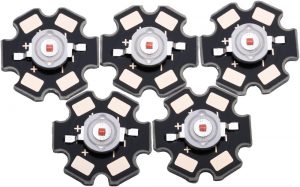
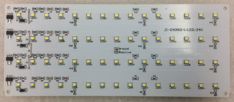
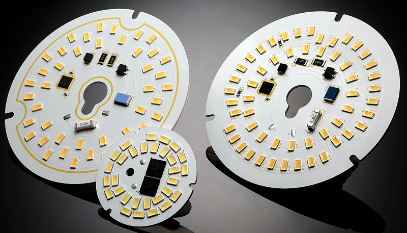
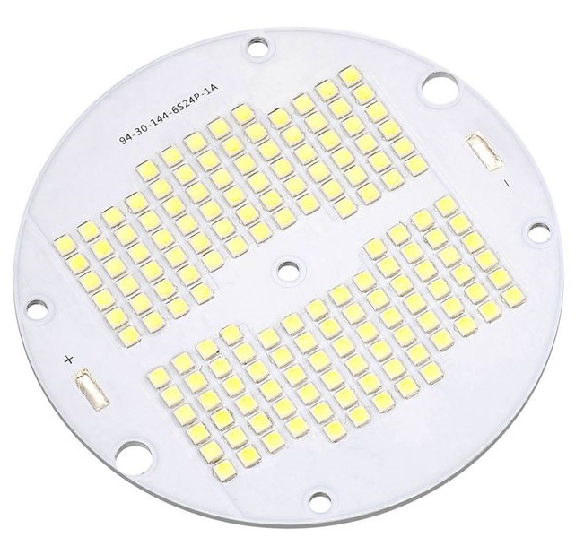
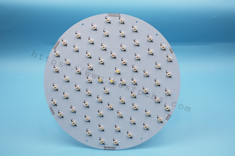
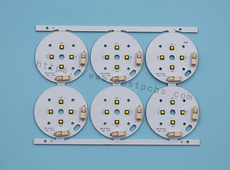
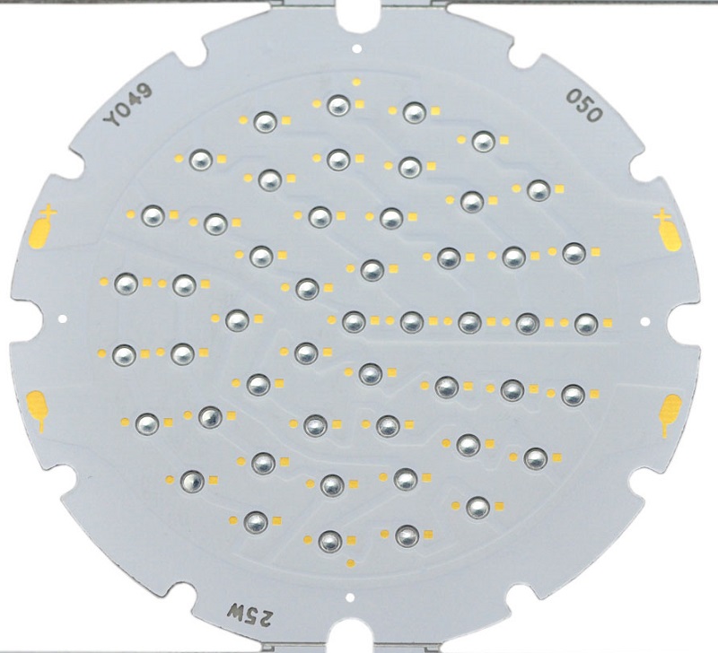
COB (Chip-on-Board) MCPCB
- Structure: LED chips are mounted directly onto the metal core PCB without individual packaging.
- Best For: High-brightness LED applications such as streetlights, automotive headlights, and stadium lighting.
- Key Benefit: Lower thermal resistance, higher efficiency, and reduced size compared to traditional LED modules.
Selecting the right MCPCB depends on your thermal management needs, power requirements, and circuit complexity. For simple applications, a single-layer MCPCB may suffice, while high-power and heat-sensitive applications benefit from SinkPAD or multilayer MCPCBs.
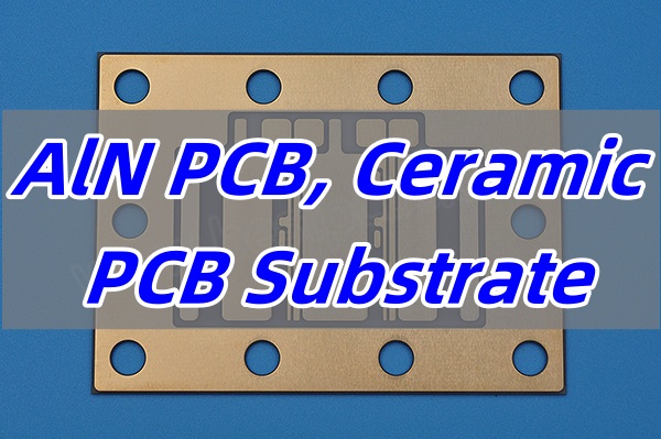
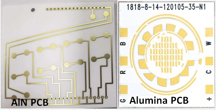
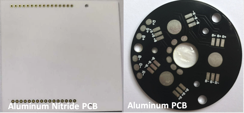
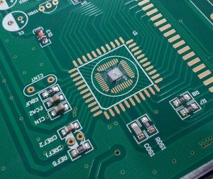
What Materials Are Used to Make Metal Core PCBs?
MCPCBs are made from a combination of conductive and non-conductive materials to ensure durability and heat dissipation. Here’s a breakdown of the materials:
- Metal Core – The base material is typically aluminum, copper, or stainless steel. Aluminum core PCBs are lightweight and cost-effective, while copper metal core PCBs offer superior heat dissipation but are more expensive.
- Dielectric Layer – This electrically insulating but thermally conductive layer separates the copper circuit layer from the metal core. It plays a crucial role in transferring heat while preventing electrical shorts.
- Copper Layer – The conductive layer where circuit traces are formed. The thickness of this layer varies based on current-carrying requirements, with heavy copper PCBs featuring thicker traces for power electronics.
The selection of metal core PCB materials depends on your design needs, thermal requirements, and budget.
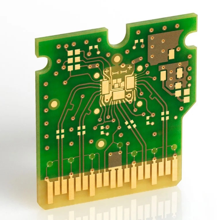
How to Design a Metal Core PCB?
Designing a metal core PCB (MCPCB) requires meticulous planning to ensure optimal performance. Here are some key considerations for designing an effective MCPCB:
Component Placement
- High-Power Components Near the Metal Core: Position high-power components close to the metal core to enhance heat dissipation and maintain thermal stability.
Thermal Management
- Thermal Vias: Incorporate thermal vias to efficiently transfer heat from the components to the metal core.
- Proper Spacing: Ensure adequate spacing between components to prevent overheating and maintain air circulation for effective cooling.
Layer Stack-up
- Bonding Strength: When designing multilayer MCPCBs, ensure robust bonding between the dielectric and metal layers to maintain structural integrity and thermal conductivity.
Trace Width and Spacing
- Wider Traces for Current Flow: Use wider traces to reduce resistance and improve current flow, especially for high-power applications.
- Adequate Spacing for Safety: Maintain sufficient spacing between traces to prevent electrical shorts and ensure safety.
Drilling and Routing
- Special Manufacturing Techniques: Due to the hardness of metal core boards, special drilling and routing techniques are required. Consult with your manufacturer to ensure compatibility with their production processes.
Design Software
- Professional PCB Design Software: Utilize professional PCB design software to optimize the manufacturing process, prevent design flaws, and ensure compliance with industry standards.
Additionally, consider the following for a comprehensive MCPCB design: - Material Selection: Choose the appropriate metal core material (e.g., aluminum, copper) based on your thermal and mechanical requirements.
- Dielectric Layer Properties: Select a dielectric layer with good thermal conductivity and electrical insulation properties.
- Antipad Application: In double-sided MCPCB designs, apply an antipad to indicate the via-hole region that requires an insulating filter to prevent electrical shorts.
As a leading metal core PCB manufacturer over 18 Years Experience, we excel in metal core PCB design. We can design a metal core PCB that maximizes performance, ensures reliability, and meets your specific application needs.
What Are the Benefits of a Metal Core PCB?
Why should you choose MCPCBs over traditional FR4 boards? Here are the key advantages:
- Superior Heat Dissipation: The metal core (e.g., aluminum or copper) rapidly absorbs and distributes heat away from components, reducing thermal stress and preventing performance degradation in high-power circuits.
- Higher Durability: MCPCBs withstand extreme temperatures, mechanical shocks, and vibrations better than FR4, making them ideal for harsh industrial or automotive environments.
- Improved Electrical Performance: Lower thermal resistance minimizes voltage drops and parasitic inductance, enhancing efficiency in high-current applications.
- Extended Lifespan: Effective thermal management reduces component fatigue, significantly prolonging the operational life of electronics.
- Compact Design: Eliminates the need for bulky heat sinks, enabling slim and lightweight solutions for space-constrained applications like LED modules or EV power systems.
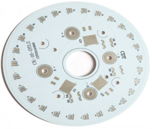
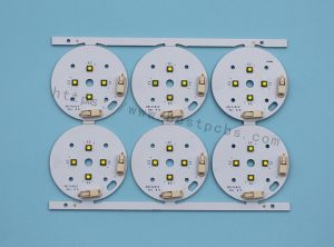
What Are the Applications of Metal Core PCBs?
Thanks to their high thermal conductivity and reliability, MCPCBs are widely used in:
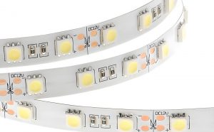
- LED Lighting: Critical for high-brightness LED applications (e.g., streetlights, automotive headlights), where they prevent overheating and ensure consistent light output and longevity.
- Automotive Electronics: Used in electric vehicle (EV) battery management systems, motor controllers, and brake systems to handle high currents and extreme temperature fluctuations.
- Power Electronics: Essential for inverters, converters, and industrial power supplies that require heavy copper layers and stable thermal performance.
- Medical Devices: Found in MRI machines, X-ray equipment, and surgical tools, where reliability and heat dissipation are critical for patient safety.
- Telecommunications: Supports high-frequency RF/microwave circuits in 5G infrastructure and radar systems, reducing signal loss caused by heat buildup.
Why Choose Best Technology as Your Metal Core PCB Manufacturer?
With so many circuit board manufacturing companies out there, why should you choose Best Technology? Here’s what sets us apart:
- 18+ Years of Experience: We specialize in metal core PCB fabrication with cutting-edge technology over 18 years.
- Wide Range of Solutions: From single-layer MCPCB to multi-layer SinkPAD board, we manufacture all types of PCBs. If you have related inquiries or questions, you are warmly welcome to contact us.
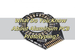
- Custom Designs: Do you need a metal core PCB prototype? We offer quick-turn prototypes tailored to your needs.
- High-Quality Standards: We use premium metal core PCB materials for better durability and performance.
FAQs of Metal Core PCB
1. What metals are in circuit boards?
- Circuit boards contain different metals depending on their type. Copper is the most common metal used for conductive traces due to its excellent electrical properties. In metal core PCBs (MCPCBs), the core is typically made of aluminum or copper to improve heat dissipation. Steel is rarely used because it’s heavier and less effective at conducting heat.
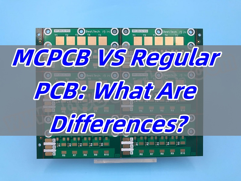
2. What is the difference between FR4 and MCPCB?
- MCPCB VS Regular PCB: What are Differences? FR4 PCBs are made from fiberglass-reinforced epoxy, offering a low-cost, durable, and electrically insulating solution. However, they have limited heat dissipation capabilities, making them suitable for applications with moderate power levels.
- MCPCBs (Metal Core PCBs) have a metal base (usually aluminum or copper) with a thermally conductive dielectric layer, allowing them to dissipate heat 5–8 times better than FR4. These are ideal for high-power applications, such as LED lighting and power electronics, where heat management is critical.
3. How are metal core PCBs laminated?
Laminating a metal core PCB involves several steps:
- Metal Base Preparation – The aluminum or copper core is cleaned and sometimes treated to improve insulation and corrosion resistance.
- Dielectric Layer Application – A thermally conductive but electrically insulating layer is applied between the metal base and the copper circuitry.
- Copper Lamination – The copper foil is bonded to the dielectric layer using high pressure and heat to ensure strong adhesion.
This process ensures the PCB can effectively transfer heat away from components while maintaining electrical insulation.
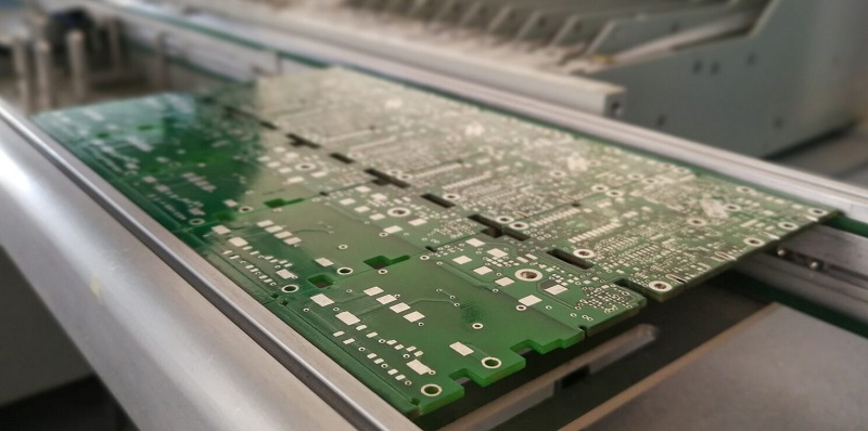
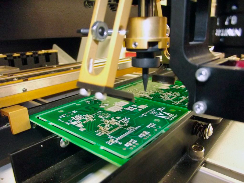
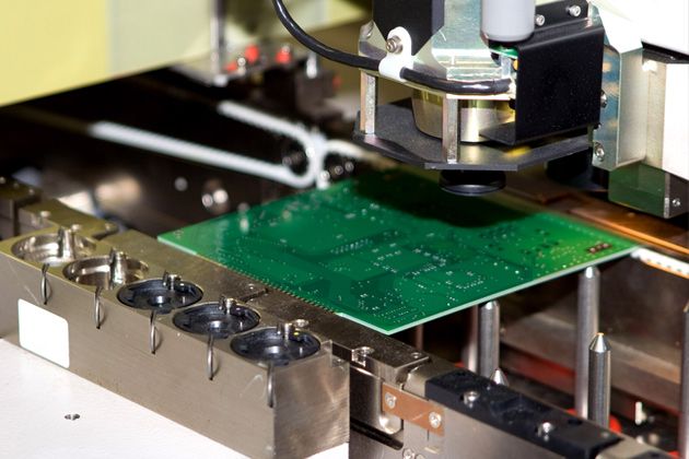
4. How to make metal core PCB?
The manufacturing process for metal core PCBs includes:
- Cutting and Cleaning the Metal Core – The aluminum or copper base is cut to the required size and cleaned to remove any impurities.
- Applying the Dielectric Layer – A heat-conductive but non-conductive layer is added to separate the metal core from the copper circuit.
- Etching the Circuit Pattern – The copper layer is coated with a photoresist, exposed to UV light, and etched to create circuit traces.
- Drilling and Plating – Holes are drilled for vias and plated with copper to establish electrical connections.
- Surface Finishing – A protective finish like ENIG (Electroless Nickel/Immersion Gold) or OSP (Organic Solderability Preservative) is applied to prevent oxidation and improve solderability.
- Testing and Quality Control – The finished boards undergo electrical and thermal testing to ensure they meet performance requirements.
This process results in a highly durable and heat-efficient PCB, making it suitable for applications that require superior thermal management.
In conclusion, metal core PCBs are the go-to solution for applications that demand superior thermal management, durability, and high performance. Whether you’re working with high-power LED lighting, automotive electronics, or power conversion systems, MCPCBs ensure stable operation under extreme conditions. With different types such as single layer MCPCB, multi layers MCPC, and advanced SinkPAD MCPCBs, designers can choose the right configuration based on their specific thermal and electrical requirements.
At Best Technology, we leverage 18+ years of experience in PCB manufacturing to deliver high-quality metal core PCBs tailored to your needs. From prototype development to mass production, we provide reliable, high-performance solutions with strict quality control. For inquiries or more info about metal core PCB, welcome to email us at sales@bestpcbs.com.