What is PCB manufacturing?PCB (Printed Circuit Board) manufacturing refers to the process of creating boards that support and connect electrical components. These boards form the foundation of modern electronics, from smartphones to industrial machines. The process involves creating conductive pathways for electronic signals, ensuring the correct components are attached in the right order and position. PCB manufacturing is a crucial industry, providing the backbone for most of today's technology. The process can vary depending on the board's complexity, materials used, and the end product's intended use.
How to choose a PCB manufacturer?Selecting the right PCB manufacturer can be challenging but is key to ensuring high-quality products. When choosing a manufacturer, consider factors like:
1. Determine Your Needs
Before choosing a manufacturer, you should first clarify your requirements:
Product Type: Define the type of PCB you need, such as single-sided, double-sided, or multi-layer boards.
Size and Layers: Specify the required PCB size and the number of layers.
Materials and Surface Treatment: Choose appropriate materials and surface treatment technologies based on your application needs.
Quality Standards: Determine the quality standards required, such as IPC-A-600 class II or class III.
2. Manufacturer Qualification Assessment
When selecting a PCB manufacturer, consider the following qualifications:
Certifications: Check if the manufacturer holds certifications like ISO9001 for quality management systems, or industry certifications like IATF19494 for automotive and ISO13485 for medical device. For those certifications, Best Technology holds them.
Experience: Assess the manufacturer's experience and expertise in the specific field or product type.
Technical Capabilities: Understand the manufacturer's technical capabilities, including production equipment and process levels.
3. Quality Control
Learn about the manufacturer's quality assurance processes, including incoming material inspection, process control, and final inspections. Evaluate the manufacturer's testing capabilities, such as functional testing and reliability testing.
4. Delivery Time and Flexibility
Delivery Schedule: Confirm whether the manufacturer’s delivery time aligns with your project requirements.
Small-Batch Production Capability: Assess whether the manufacturer can accommodate small-batch orders flexibly.
5. Costs
Price Comparison: Obtain quotes from multiple manufacturers and perform a cost analysis.
Long-Term Cooperation Potential: Consider establishing a long-term partnership with the manufacturer for better pricing and services.
How is a PCB manufactured step by step?PCB manufacturing process is different for different PCB factories, different layers of PCB, but some steps are same and all of them will have to do. Single layer PCB and Double layers PCB are all use the raw material so that they don't need to do Lamination process, they are easy to do. So here we will show 4 layers PCB manufacturing process as multilayer PCB.
Usually we fabricate 4 layers PCB as the following stackup, and we will show the manufacturing process as this 4 layers PCB. But here won't all the step just show some important step which can help you to know how we manufacture PCB, because it will make you lost if we list all the steps. But don't hesitate to contact if you need more information, we are always here for you.
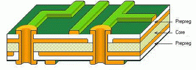
1. Cutting Sheet
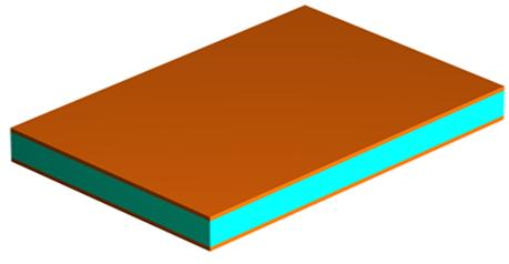
We have to cut a small size board from the big raw material, assume we will manufacture a PCB with the size 10 mm * 10 mm. As the following picture, you will find the raw material include two copper layers that will be final layer 2 and layer 3, and both are inner layer.
2. Chemical Clean
To get good quality of the etched pattern, and make sure the combination between corrosion resistant layer and substrate surface is strong, so the substrate surface must be without oxidation layer, oil, dirt, fingerprints, and other contaminants. So we need to do chemical clean.
3. Inner Layers
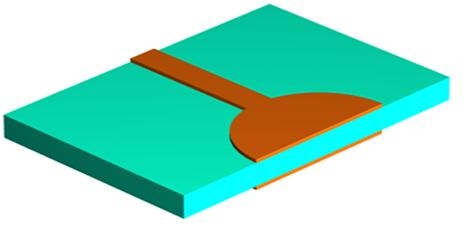
Circuit layer is a complex process, including Dry Film Lamination, Expose, Develop and Copper etching.
4. Lamination
After inner layers, we will laminate so that we can get a 4 layers structure from 2 layers structure.
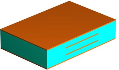
5. CNC Drilling
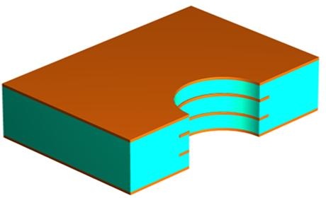
6. Plated Through Hole
After lamination and drilling, we get a 4 layers structure, but we need to do plated through holes to connect different layers.
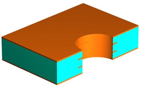
7. Outer Layer
After plated through holes we will do outer layer now like inner layers, but you will find we do Tin Pattern Electro Plating to protect copper layers, but will strip Tin after Copper Etch.
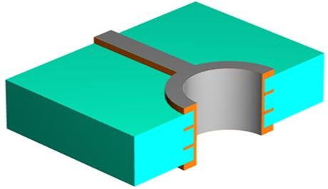
8. Solder mask
Solder mask is used to protect the copper layers meanwhile avoid short circuit when SMT and weld.
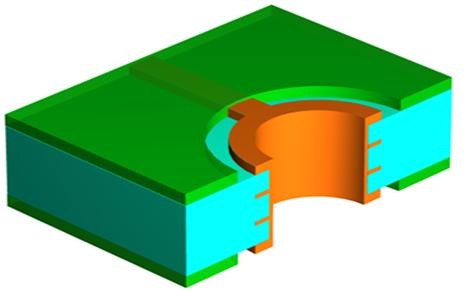
9. Surface Finishing
PCB surface finishing includes HASL, OSP, ENIG and so on, which is protect pads and prolongs the self left, because it may take long time before we do SMT or weld.
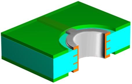
10. Outline
After solder mask and surface finishing, at last we need V-Cut or Routing to make the final outline meet PCB files.
11. FQC, Packaging and Shipping
After outline, we will check the final PCB quality, package and ship to customers.
Now you may know how to fabricate PCB in our workshop, meanwhile we also welcome you to our factory to see more details, and please let us know if you would like to order PCB, Best Tech will be your best choice.
How long does it take to manufacture a PCB?The time it takes to manufacture a PCB depends on various factors such as complexity, quantity, and the manufacturer’s capabilities. For simple PCBs, production can be completed in as little as 24 to 48 hours. However, for more complex boards with multiple layers or specific material requirements, the process can take several weeks. The average timeline for a standard board is usually 5 to 7 days. Expedited services are available for those who need faster delivery. Here is Best Technology capabilities with prototype and mass production lead time:
What is the standard for PCB manufacturing?The standard for PCB manufacturing revolves around a series of international certifications and guidelines that ensure the product’s quality, safety, and environmental compliance. Some key standards include:
1. Quality standards
In the circuit board production process, there must be a series of quality standards to ensure that the products produced meet customer requirements, while ensuring product consistency and stability. Commonly used standards are ISO, IPC, UL and so on.
ISO as an international quality management standards development organization, its ISO9001 series standards are globally recognized quality management standards. In the field of circuit board manufacturing, IATF/TS16949 is a widely used standard that describes how to meet international quality management standards in the manufacture of electronic products, including research and development, production, installation and service activities. IPC is the abbreviation of the Electronic Industry Alliance Committee (Institute of Printed Circuit Boards), IPC standards are mainly to ensure the process level and quality stability of the circuit board manufacturing industry, of which the most widely usedIPC-A-600is A standard on acceptability standards. The degree and acceptability of various surface defects of circuit boards are specified. UL, short for Underwriters Laboratories, is an important standard for circuit board production and end product certification to ensure that the circuit board meets the safety and reliability requirements of electronic devices in the market.
2. Environmental standards
Another important factor to consider in the board production process is environmental standards. Environmental standards focus on environmentally friendly design throughout the product life cycle, ensuring that products are not harmful to the environment and meet the needs of sustainable development, and reduce the negative impact on the environment during production. The main environmental standards include ISO 14001, RoHS, etc. ISO 14001 is a standard issued by the international standards organization ISO, which is an environmental management system standard that can help organizations optimize their environmental performance, by implementing this standard, circuit board manufacturers can ensure the implementation of environmental management, including reducing the use of energy and materials, reducing waste generation and so on. RoHS is the EU's Restriction of Hazardous Substances directive, including lead, mercury, cadmium, hexavalent chromium, polybrominated biphenyls and polybrominated diphenyl ethers and other six hazardous substances. In the circuit board manufacturing industry, the RoHS directive imposes restrictions on all electronic products, including circuit boards.
3. Safety standards
Circuit boards are an important part of electrical products, so safety standards are also an essential part of the manufacturing process. Safety standards mainly cover electrical safety, safety certification, fire protection and explosion safety. The main safety standards include IEC, CE, etc. IEC Standards is an international standards organization, among which IEC 60601 is a safety standard for medical electrical equipment, covering requirements such as voltage resistance and insulation performance. CE standard is a sign of the European Community, representing free trade in the EU market, no tax and other special treatment. The CE standard is for the electromagnetic compatibility and safety requirements of products, to ensure that the products sold in the EU market are safe and reliable, and meet the relevant safety standards.
What certifications are Needed for PCB manufacturers?PCB manufacturers must meet a variety of certifications to prove their competence and reliability. Some of the essential certifications include:
UL certification – for safety of product
IPC certification - especially IPC-A-600 and IPC-6012
RoHS – environment standard
ISO9001 – quality control system
ISO14001 – environmental management system
IATF 16949 – for automotive electronics
ISO13485 – for medical industry
What files are required for PCB manufacturing? To manufacture a PCB, certain files must be provided to the manufacturer to ensure accurate production. These files include:
Gerber file (RS-274-X format)
Aperature/D code file
NC Excellon Drill File
Drill Tool list (if not listed in NC Drill file)
Soldermask
Silkscreen
Readme.txt file
BOM file
Pick and place files
Quantity for prototype
Quantity for volume production
Which files do PCB manufacturers Accept?Most manufacturers acceptGerber filesand drill files, as these are the standard for PCB production..dxf or .dwgfiles also available in Best Technology. In addition, they may request other files such as the BOM and Pick and Place files, depending on the level of assembly they are responsible for.
Which gerber files are needed for single-sided PCB manufacturing? For single-sided PCBs, you typically need fewer files than for multi-layer boards. The necessary files include:
Top Copper Layer Gerber File: The design of the copper traces.
Drill File: The location of the holes.
Solder Mask File: This file is needed to define the areas that will be soldered.
Silkscreen File: This file indicates the component labels and markings.
If it requires to do PCB assembly service, two extra layers should include:
Stencil file: The stencil layer is used to define the position and size of the soldering points.
BOM file: With each component information
Pick and place file: For assembly usage
These files are essential for single-sided PCB production.
In addition to this, here are some common terms used in Gerber files:
GTL: indicates the top layer.
GBL: Bottom layer.
GTO: indicates the top overlay.
GBO: indicates the bottom overlay.
GTP: indicates the top paste.
GBP: indicates the bottom paste.
GTS: indicate top solder (also called solder/green oil, negative).
GBS: Bottom solder.
G1, G2, ...: indicates the internal cabling layer, for example, G1 indicates the first internal cabling layer, and G2 indicates the second internal cabling layer.
GP1, GP2: indicates the Internal Plane.
GM1, GM2: Mechanical Layer.
GKO: indicates that the KeepOuter layer is prohibited.
GG1: indicates the drill guide.
GD1: indicates drill drawing layers.
GPT: indicates the top pad master.
GPB: indicates the bottom pad Master.
How does copper weight impact PCB manufacturing? Copper weight refers to the thickness of the copper layer on a PCB. It affects the board's ability to carry current and dissipate heat. Thicker copper layers are used for high-power applications, while standard copper weights are sufficient for most electronic devices.
The correct copper weight and thickness can ensure the quality and performance of the circuit board, but also affect the reliability and stability of electronic products. Copper thickness determines the conductive effect of the circuit board, if the copper layer is too thin, it may lead to decreased conductive performance, signal transmission interference and loss, thus affecting the performance and reliability of the PCB. On the contrary, if the copper layer is too thick, although the conductivity will be very good, it will increase the resistance value of the circuit board, so that the signal transmission is hindered, and it will also increase the cost and manufacturing difficulty of the circuit board.
In addition, the inner copper thickness also has a significant impact on the processing difficulty of the PCB. The inner layer of copper thickness is too thick will lead to the PCB processing difficulty increases, such as drilling and milling and other processing processes become more difficult and complex, thus increasing the manufacturing cost and lead time.
When are PCBs drilled during manufacturing? Drilling occurs after the copper layers are etched. This step is crucial for creating holes for components and vias that connect different layers in multi-layer boards. The precision of the drilling process is vital for ensuring proper alignment and electrical connectivity. Drilling happens early in the production process, allowing the board to be plated and further processed.