EBest Circuit (Best Technology) is your top choice for PCB assembly services in Asia, offering full turn key solutions to meet all requirements of your project. Our SMT assembly services are highly precise and efficient, ensuring accurate placement of a wide range of components, from standard resistors to complex integrated circuits. We excel in Press-fit technology assembly, demonstrating our skilled expertise in handling complex components. Whether you are in prototyping or ready for mid-scale production, our services are designed to seamlessly meet your various needs.
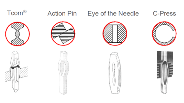
Press-fit technology, originating in the 1970s, has evolved significantly over the decades. With the continuous advancement of electronic technology and the changing market demands, Press-fit technology has gradually been widely applied. From the initial rigid press-fit to the later flexible press-fit, such as C-press, Eye of the Needle, and Tcom press-fit sections, the technology has been continuously improved and perfected. In the 21st century, Press-fit technology has been extensively used in industries like telecommunications, automotive, locomotives, military, and automation equipment, especially in connectors, where it has become very popular.

Press-fit technology is a solderless connection technique widely applied across several fields, such as automotive, telecommunications, computers, and automation equipment. It involves inserting a specially designed pin into a plated-through hole (PTH) in a printed circuit board (PCB) using mechanical pressure, forming a secure and reliable electro-mechanical connection. This process functions similarly to a blade-and-socket connector pair, but with the genders reversed: the press-fit pin acts as the "blade" with flexible beams, while the PCB hole remains rigid.
The critical forces in this connection are the Normal Force and the Insertion Force. The Normal Force is the pressure the press-fit pin exerts on the walls of the PCB hole, ensuring a stable electrical connection. The Insertion Force is the resistance the PCB hole exerts on the pin during insertion. Unlike blade-and-socket connectors designed for repeated connections and disconnections, press-fit joints are more permanent, necessitating higher Normal Force for a stable connection
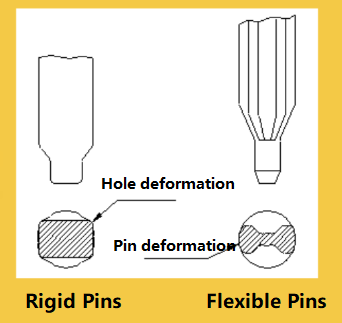
There are two types of press-fit parts:
l Rigid/Solid pins: These do not deform during insertion, making them suitable for applications where the connection needs to remain robust and stable, such as in multi-layer PCBs.
l Flexible pins: These deform when inserted into the PCB through-hole, making them more adaptable and reducing the risk of damaging the PCB or the plating within the hole.

Among the two methods, flexible pin technology is more suitable for press-fit connections. Rigid pins are mainly used in multilayer printed circuit board technology, providing electromechanical connections at the top end of each PCB. Flexible pin press-fit technology has several advantages over rigid pin technology:
l It mitigates potential damage to the PCB's plated-through holes.
l It allows for greater tolerance in the diameter of the holes.
l It reduces the insertion force, making the assembly process easier and more reliable.
l It permits multiple insertions and removals, enhancing the flexibility and reusability of the PCB.
Compared to traditional soldering techniques, Press-fit technology offers several significant advantages:
1. No thermal stress
The press-fit process does not require heating, so it does not generate thermal stress on the PCB or components, which is beneficial for protecting sensitive components and circuit structures.
2. No soldering defects
It avoids common soldering issues like cold joints, shorts, and insufficient solder, improving the reliability and stability of connections.
3. No flux residue
The press-fit process does not require flux or cleaning agents, preventing the creation of conductive residues and maintaining the cleanliness and electrical performance of the circuit board.
4. Efficiency and cost-effectiveness
The press-fit process simplifies production, increases efficiency, and reduces production costs and energy consumption.
5. Reusability
Press-fit connectors can be repeatedly assembled and disassembled without damage, which enhances the maintainability and flexibility of the product.
6. Environmental and safety compliance
Without the use of solder or cleaning agents, the process reduces the release of harmful substances and environmental pollution, meeting modern manufacturing's environmental requirements.
The choice of materials is crucial for the success of press-fit technology. The pins, typically made from copper alloys or stainless steel, must offer excellent mechanical and electrical properties. Common materials include:
l Copper Alloys: Known for their good conductivity and workability, examples include bronzes (e.g., CuSn4/C511, CuSn6/C519) and CuNiSi alloys (e.g., C7025).
l PCB Metallized Holes: These are generally coated with copper. The plating must be uniform and burr-free, with sufficient thickness to ensure reliable and stable press-fit connections.
The PCB itself must be designed to withstand the thermal and mechanical stresses associated with press-fit processes. Proper hole construction and material selection are essential to prevent issues such as delamination or increased contact resistance over time
To ensure the correct functioning of a press-fit connection, the PCB hole construction and materials are of paramount importance. The PTH must have appropriate copper thickness and be free of defects like burrs or uneven plating. If the raw hole is drilled too large and then filled with copper, over time, the copper may push away, leading to increased contact resistance. Conversely, if the hole is too small or the copper too thin, the copper can be pushed out or delaminate from the internal layers during the press-fit process.
PCB materials must also be selected to meet the thermal requirements of the application. For example, in automotive applications, the PCB’s glass transition temperature (Tg) should exceed the operational temperature by a safe margin to prevent the PCB from softening during operation, which could weaken the press-fit connection and increase contact resistance.
The Press-fit process is relatively simple, but each step must be precisely controlled to ensure connection quality. The general steps are as follows:
1. Preparation
l Clean the PCB: Make the PCB surface is free of oil, dust, and other contaminants.
l Check the metallized holes: Ensure the metallized holes have uniform plating and are defect-free.
l Pretreat the pins: Clean and deoxidize the pins to ensure their surface is free of contaminants and oxides.
2. Positioning and alignment
Use automated equipment or manual tools to position and align the components with the PCB. Ensure that the pins are accurately aligned with the metallized holes on the PCB. The precision of this step is crucial for the success of the subsequent press-fit, as any slight deviation may lead to poor connections or damage.
3. Press-fit operation
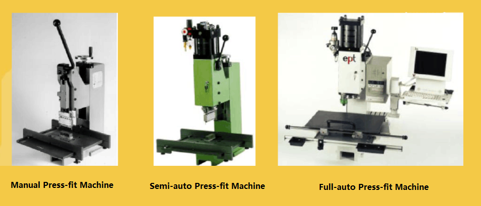
l Choose the appropriate press-fit equipment and die. The press-fit equipment must provide sufficient pressure while maintaining a stable press-fit speed and time.
l Install the press-fit die on the equipment and place the PCB under the die.
l Start the press-fit equipment, applying pressure to the pins and pressing them into the PCB's metallized holes. During the press-fit process, closely monitor parameters like pressure value, press-fit time, and insertion depth to ensure tight and stable connections.
l After the press-fit is completed, check the connection for firmness, ensuring there is no looseness or breakage.

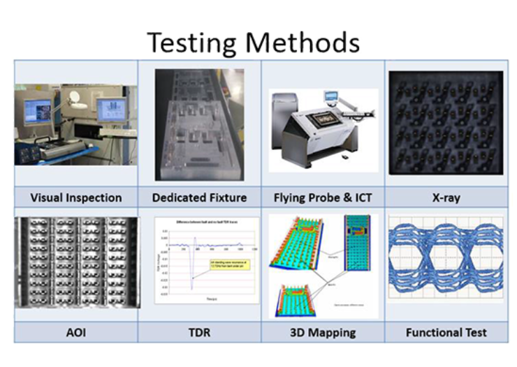
4. Quality inspection
a). Visual inspection: Check the press-fit points for visible deformation, cracks, or damage.
b). Electrical performance test: Use testing instruments to check the electrical performance of the connection, including contact resistance, insulation resistance, and voltage withstand parameters.
c). Mechanical performance test: Evaluate the mechanical strength and durability of the connection through vibration and shock tests.

5. Post-processing
Although the Press-fit process does not require cleaning of flux and residues, it may require other types of cleaning to remove micro-particles or contaminants generated during the press-fit process. Then assemble the press-fitted PCB with other components or parts to form a complete electronic product.
In our SMT assembly process, Press-Fit technology is typically applied to connectors and other components that require robust, high-density connections. This technology is particularly popular in automotive electronics, telecom infrastructure, medical devices, and other high-reliability sectors.
Press-Fit connectors are also ideal for multi-layer PCBs, where a strong and stable connection is essential across various layers of circuitry. By using this technology, we ensure that our products meet the highest standards of performance and durability, especially in critical applications where failure is not an option.