Best Technology Co.,Ltd
- +86-755-2909-1601
- sales@bestpcbs.com
Low-temperature co-fired ceramic (LTCC) technology involves creating a high-density multilayer interconnected circuit board by printing conductive metal patterns onto ceramic green tapes with interconnecting through-holes, aligning them precisely, stacking them together, and finally co-firing them at 900°C to form a unified, three-dimensional circuit substrate. This process can also incorporate embedded passive components within the circuit.
LTCC technology allows embedding passive components within the inner layers of the substrate. This frees up more surface area for mounting active devices and laying out large ground planes. It provides two advantages:
1. The assembly density is increased, improving production efficiency and system reliability.
2. The large ground plane design enables excellent microwave grounding, further enhancing high-frequency performance.
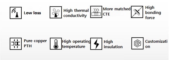
Compared to traditional PCBs, LTCC ceramic PCB offers better thermal conductivity, making it suitable for handling high current and high-temperature requirements. It also reduces the thermal stress between bare chips and the substrate during installation, facilitating easier mounting and removal.
LTCC technology increases wiring density, shortens interconnection distances, and allows independent circuit designs on different substrate layers. This satisfies the needs for miniaturization, high density, multi-functionality, high reliability, and high transmission rates in electronic systems.
It also provides excellent temperature characteristics, such as a small thermal expansion coefficient and low dielectric constant temperature coefficient. This allows the creation of very high-layer circuit boards with fine line widths smaller than 50μm.
The conductors used are highly conductive metals, which help improve the circuit system's quality factor.
LTCC production is a discontinuous process, allowing inspection of each layer before co-firing, which helps improve substrate quality and yield, shorten production cycles, and reduce costs.
The LTCC process mainly includes the preparation of green ceramic tapes, pre-treatment before punching, punching, hole filling, conductor layer printing, lamination, isostatic pressing, cutting, degassing and sintering, soldering, and testing:
1. Slurry Preparation
The material typically consists of ceramics, glass powder, and organic binders mixed according to specific formulations to create a homogeneous slurry with uniform properties.
2. Tape Casting
The slurry undergoes defoaming, and then tape casting forms the green ceramic tape. Requirements for the tape include density, uniform thickness, and sufficient mechanical strength.
3. Sheet Cutting
The tape is cut into sheets of a specified size, slightly larger than needed to allow for subsequent processing.
4. Punching
Via holes are mechanically or laser-punched into the green tape for electrical interconnection. The accuracy of the hole size and position directly impacts wiring density and substrate quality. Punching creates through-holes with diameters of 0.1-0.5 mm.
5. Hole Filling
Via holes are filled with a filler, creating vertical paths for electrical connections between layers in the multilayer ceramic substrate.
6. Printing
Conductive pastes or dielectric materials are screen-printed onto the green tape to form electrical interconnection lines and passive components such as resistors, capacitors, and varistors.
7. Lamination
The printed green sheets are stacked in a mold designed with alignment pins to ensure precise layer alignment.
8. Isostatic Pressing
The stacked green body is hot-pressed under controlled temperature and pressure conditions to ensure uniform lamination and prevent delamination during sintering.
9. Cutting
The large green ceramic substrate is cut into smaller components or modules before sintering.
10. Degassing and Sintering
The green substrates are placed in a sintering furnace, where they are gradually heated to about 850-900°C. The sintering process eliminates gases and fuses particles, ensuring proper bonding and mechanical strength.
11. Soldering
Cleaned workpieces are assembled and soldered together by heating the solder to a molten state, allowing it to bond with the metal parts.
12. Testing
The sintered LTCC multilayer substrates are tested for connectivity and functionality using probe testers, laser trimming equipment, and sorting devices.
LTCC technology enables the production of both single-function components (such as resistors, inductors, antennas, duplexers, and filters) and complex RF front-end modules that integrate antennas, switches, filters, duplexers, LNAs, and power amplifiers. These RF front-end modules help reduce the weight and size of products while achieving low power consumption. As 5G communication frequencies rise, antennas and RF modules become smaller and more integrated. At frequencies above 30 GHz, antenna sizes shrink to millimeter scale or smaller, necessitating a shift from single antennas to array antennas to improve communication efficiency.
Here are some typical applications of LTCC ceramic PCB:
l Communication devices like smartphones, iPads, and computers
l Electronic components
l Power base stations
l Automotive electronics
l Solar power applications
l Voltage regulators, amplifier circuits
l Memory modules
l Radar systems
l Aerospace and aviation
l High-frequency microwave devices
ISimply drop your email or phone number in the contact form, and we'll promptly provide you with a quotation.