EBest Circuit (Best Technology) Co.,Ltd
- +86-755-2909-1601
- sales@bestpcbs.com
What is hdi pcbHdi pcb meaning, HDI PCB is the abbreviation of high-density interconnect printed circuit board, that is, high-density interconnect circuit board, which is a printed circuit board with high integration, high precision and miniaturization.It uses advanced manufacturing technology to assemble multiple electronic components tightly together to achieve fast transmission and efficient heat dissipation of the circuit. HDI circuit board adopts micro-hole filling, metallized hole and other technologies to achieve high-speed signal transmission and high reliability; advantages of hdi pcb1. Higher integration: HDI PCB adopts tighter wiring design and smaller line spacing/line width, so that more electronic components can be accommodated on the circuit board, achieving higher integration. This means that under the same board size, HDI PCB can accommodate more functions and complex circuit designs, further improving the performance of the product.2. Better electrical signal transmission performance: HDI PCB adopts shorter circuit paths and smaller impedance, which can reduce signal transmission delay and loss, and improve the stability and reliability of electrical signals. This is crucial for the application of high-speed data transmission and high-frequency electronic devices, which can ensure signal quality and data transmission speed. 3. Higher reliability and stability: HDI PCB adopts a higher level of compression process and packaging technology, which can provide better electrical isolation and mechanical support between board layers, reduce the possibility of mutual interference and mechanical damage between electronic components, and thus improve the reliability and stability of the product. 4. Smaller size and weight: HDI PCB can significantly reduce the size and weight of the circuit board through a more compact design and multi-layer wiring. This is very important for the trend of modern electronic devices to pursue thinness and shortness. 5. Higher production efficiency: HDI PCB adopts advanced manufacturing processes such as laser perforation, thin film transformer, cover plate packaging, etc., which can achieve high-efficiency production. Compared with traditional multi-layer PCB boards, HDI PCB production process is simpler and easier to achieve automated production, thereby improving production efficiency and reducing costs. What are the disadvantages of HDI PCB?1. Signal integrity issues: As the density of integrated circuits increases, the signal integrity issues faced by HDI PCBs become more and more serious. High-density wiring can lead to problems such as electromagnetic interference (EMI) and crosstalk, which can affect the performance and reliability of electronic devices. 1.2. Difficulty in making tiny apertures: The aperture of HDI PCBs is very small, usually below 0.1mm, which makes it very difficult to make tiny apertures, increasing the complexity and cost of manufacturing. 1. 3. Material selection issues: Since HDI PCBs need to withstand harsh environments such as high temperature and high humidity, it is very important to choose the right material. The right material can not only ensure the performance and reliability of HDI PCBs, but also extend their service life. However, it is not easy to find a material that meets all requirements at the same time, which increases the difficulty of material selection. 4. High manufacturing cost: Since the manufacturing process of HDI PCBs is complex, high-precision process control and advanced manufacturing equipment are required, all of which lead to relatively high manufacturing costs. What is HDI material?1. Substrate: The substrate is the basis of HDI PCB. Commonly used organic insulating materials include thermosetting resins (such as phenolic resins and epoxy resins) and thermoplastic polyesters (such as polyimide and polytetrafluoroethylene). The choice of substrate depends on the needs of specific applications, such as rigid or flexible PCBs.2. Copper foil: As a conductive material, the thickness of copper foil is generally between 0.3mil-3mil. The specific choice depends on the current carrying size and etching accuracy. The quality of copper foil directly affects the surface quality and electrical performance of the product. 3. PP (B-stage resin): When making multi-layer PCBs, PP is an indispensable material as an interlayer adhesive. 4. Photosensitive materials: Including photoresists and photosensitive films, divided into wet films and dry films. These materials will undergo chemical changes under light of a specific wavelength, affecting their solubility in the developer, thereby achieving precise production of circuits. 5. Solder mask (ink): As a solder mask, solder mask is used to prevent the adhesion of liquid solder, and its performance affects the welding quality and circuit protection of PCBs. 6. Film: Similar to the polyester film used for photography, the film is used to record image data and requires high contrast, sensitivity and resolution while ensuring fine lines and dimensional stability. What is HDI flex pcbHdi flex pcb is a product that combines high-density interconnection technology (HDI) and flexible circuit board technology.HDI technology is mainly used for circuit boards with dense lines, high layers, and drilling holes less than 0.15mm. It is manufactured by adding layers and micro blind holes, and supports various forms of 1st and 2nd order arbitrary interconnection. This technology enables circuit boards to achieve more sophisticated wiring, tighter interlayer connections, and more reliable electrical performance. Flexible circuit boards are circuit boards that can be bent and folded. They are flexible and foldable, and are suitable for application scenarios that require flexible wiring and limited space. hdi multilayer pcbHDI multilayer circuit board, full name High-Density Interconnect PCB, is an advanced printed circuit board (PCB) that uses high-density interconnect technology to allow more circuit connections in a very small space. The emergence of this technology is mainly to cope with the trend of electronic products towards miniaturization, multi-function and high performance.HDI PCB Classification1. Classification by dielectric material:Laminated multilayer boards made of photosensitive materials, with photosensitive resin filled in the substrate. Laminated multilayer boards made of non-photosensitive materials, with no photosensitive resin in the substrate, are mostly high-temperature resistant FR-4 substrates or other heat-resistant substrates. 2. Classification by micro-via formation process: Laminated multilayer boards with photoinduced hole formation, with micro-vias formed by photoimaging-etching. Laminated multilayer boards with plasma bombardment hole formation, with micro-vias formed by plasma bombardment. Laminated multilayer boards with laser hole formation, with micro-vias formed by drilling with CO2 laser or UV-YAG laser. Laminated multilayer boards with chemical hole formation, with micro-vias formed by chemical etching. Laminated multilayer boards with mask-protected jet sandblasting hole formation, with micro-vias formed by mask-protected jet sandblasting. 3. Classification by electrical interconnection method: Multilayer boards interconnected by electroplating micro-vias, the interconnected micro-vias are formed by electroplating. HDI boards formed by filling conductive paste, the interconnected micro-vias are formed by filling conductive paste. 4. Classification by application scope: Boards for mobile communication equipment and notebook computers, characterized by a large number of holes, light volume, short, small, and strong functions. Boards for high-end computers and network communication equipment and their large peripherals, characterized by a small number of holes, a large number of wire layers, and the requirements for the integrity of the transmission signal and characteristic impedance control. Chip carriers for large-scale integrated circuit packaging, including press-bonded boards (also known as wire bonding boards) and flip-chip boards (flip chips), are characterized by small line width and spacing, high precision, small aperture, small hole spacing, good heat resistance of the substrate, and small thermal expansion coefficient. hdi pcb manufacturing process1. Design stage: Design the circuit diagram according to customer needs, determine the board layer structure and stacking method.2. Material preparation: Select substrate materials, copper clad films, covering layers and internal layers that meet relevant standards to ensure product quality. 3. Laser drilling: Use laser technology to process small holes on the board to achieve circuit connection. 4. Pressing stage: The inner and outer layers of the board are cured through a hot pressing process to become a compressed circuit board to ensure the tightness and stability of the circuit board. 5. Etching stage: Remove the unnecessary parts of the copper clad film through chemical methods to retain the required conductive path. 6. Plating stage: Electroplating the board surface to give it good conductivity and anti-oxidation properties. 7. Plug-in stage: Insert the components into the circuit board and fix them by welding. 8. Testing stage: Ensure the quality and performance of the product through strict testing and inspection. hdi pcb manufacturerOur products ranging from standard hdi pcb, hdi flex pcb,2-16 layer hdi multi-layer pcb,any layer hdi pcb and rigid-flexible PCBs to high frequency PCBs.hdi pcb factory, Currently our mouthy capability is 260,000 square feet (28,900 square meter), more than 1,000 different boards will be completed. We also provide expediate service, so that urgent boards can be shipped out within 24 hours.At a custom printed circuit board manufacturer, we believe that continuous growth is the key to success. So, we always invest much in research and development to stay ahead of industry trends. Our focus on product quality and customers satisfaction, and we aim to build strong relationships and offer personalized support and solutions to our customers. hdi pcb prototypeBest pcb is a professional PCB manufacturer, dedicated to high-end HDI, multi-layer PCB, HDI quick board proofing, PCB proofing, PCB fast proofing, high-frequency PCB, high-speed PCB, FPC, soft and hard board, SMT processing and PCBA OEM. We provide one-stop PCB and PCB manufacturing services, not only with fast delivery but also with competitive prices. We always provide customers with cost-effective and inexpensive PCB and PCB products.hdi pcb design guidelines1. Stacking structure design: The wiring efficiency of HDI PCB depends on its stacking structure, including the design of signal layer, power/ground layer, and vias.2. Via technology: One of the core features of HDI PCB is micro-via technology, which requires precise design to accommodate inter-layer wiring. Via size and type directly affect the manufacturing process and performance of the circuit board. The ball pitch of the BGA component will determine the via size used, which in turn affects the selection of HDI manufacturing process. 3. Component placement: In HDI layout, trace width, via size, and BGA component placement/avoidance routing are the key considerations. Optimizing component layout can not only improve routing efficiency, but also reduce manufacturing difficulty. 4. Signal integrity: As electronic devices move towards higher frequencies and smaller sizes, signal integrity becomes an important consideration. Using low dielectric constant PCB materials helps maintain signal integrity and stability, especially when implementing a large number of high-speed digital interfaces. 5. Manufacturing process: The manufacturing process of HDI PCB involves multiple special steps, including the use of special materials and processes to ensure the accuracy of micro-vias and the tight arrangement of wiring. Working closely with the board manufacturer to confirm their manufacturing methods and limitations is key to ensuring the feasibility of your design. High Density Interconnects (HDI) board are defined as a board (PCB) with a higher wiring density per unit area than conventional printed circuit boards (PCB). They have finer lines and spaces (<100 µm), smaller vias (<150 µm) and capture pads (<400 µm), I/O>300, and higher connection pad density (>20 pads/cm2) than employed in conventional PCB technology. HDI board is used to reduce size and weight, as well as to enhance electrical performance. According to layer up different, currently DHI board is divided into three basic types: |
|
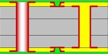
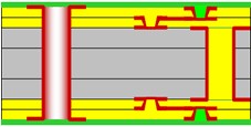
1) HDI PCB (1+N+1) Features:
Application: Cell phone, UMPC, MP3 Player, PMP, GPS, Memory Card 1+N+1 HDI PCB Structure: |
|
 |
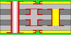 |
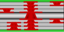
2) HDI PCB (2+N+2) Features:
Application: Cell phone, PDA, UMPC, Portable game console, DSC, Camcorder |
|
 |
 |
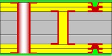
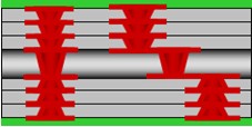
3) ELIC (Every Layer Interconnection) Features:
Application: Cell phone, UMPC, MP3, PMP, GPS, Memory card.
|
|
 |
 |
| Click here for information about the Flowchart of HDI Board. | |
| Please click here for immediate quotation online Please contact us for more information about HDI Board. |
|
ISimply drop your email or phone number in the contact form, and we'll promptly provide you with a quotation.