EBest Circuit (Best Technology) Co.,Ltd
- +86-755-2909-1601
- sales@bestpcbs.com
If you’ve worked with high-frequency circuits or sensitive signals, you might have come across the term “impedance control.” Understanding and managing impedance can be the difference between a reliable design and one plagued by signal loss or interference.
Impedance, in simple terms, is the opposition a circuit offers to the flow of alternating current (AC). It combines two elements: resistance, which is straightforward opposition, and reactance, which is the opposition due to capacitance and inductance. Together, they form impedance, usually measured in ohms (Ω).
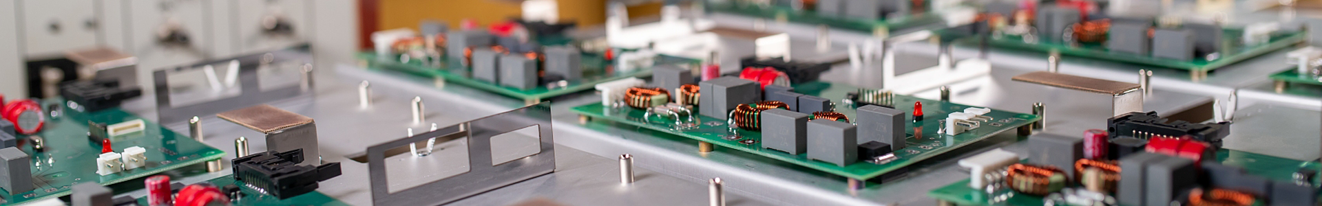
In a PCB, impedance is vital because it affects how signals propagate through the traces. If the impedance isn’t controlled, it can lead to reflections, signal loss, or even total communication failure, especially in high-speed circuits.
Impedance control refers to the process of designing PCB traces to have specific, predictable impedance. It’s not just about ensuring the impedance is low but that it is consistent and matches the system's requirements. In high-speed digital and RF circuits, where signals are transmitted at high frequencies, impedance control becomes essential to avoid issues like signal degradation or electromagnetic interference (EMI).
The goal of impedance control is to maintain the signal's integrity as it travels through the PCB. By controlling impedance, designers ensure that signals reach their destination without significant loss or distortion.
When one parameter varies while keeping other conditions constant, the factors affecting impedance are as follows:
Trace Width
The width of the trace affects its resistance and inductance. Wider traces generally have lower resistance, which in turn reduces the impedance. However, this also increases the capacitance between the trace and the reference plane, which can complicate impedance control. The width must be carefully calculated to balance these effects and achieve the desired impedance.
Trace Thickness
The thickness of the copper trace influences its resistance. Thicker traces, like wider ones, lower resistance and thereby reduce impedance. However, increasing the thickness also impacts the trace's ability to carry current. The trade-off between trace thickness and other design constraints must be carefully managed.
Dielectric Constant (Dk)
The dielectric constant of the material affects the capacitance between the trace and the reference plane. Different board materials have distinct dielectric constants, which are related to the resin materials used. For instance, FR4 board materials have dielectric constants ranging from 3.9 to 4.5, decreasing with increasing frequency. PTFE board materials have dielectric constants ranging from 2.2 to 3.9.
Dielectric Thickness
The thickness of the dielectric layer between the trace and the reference plane also impacts impedance. The thicker the dielectric, the higher the impedance. A thicker dielectric layer reduces capacitance, thereby increasing impedance. Conversely, a thinner layer increases capacitance and reduces impedance.
Loss Tangent
The loss tangent (or dissipation factor) of the dielectric material represents how much signal energy is lost as heat. Materials with a lower loss tangent are preferred in high-frequency applications because they preserve signal integrity better, thereby maintaining consistent impedance.
Coupling and Crosstalk
When traces are placed too close to each other, coupling occurs, leading to crosstalk, where a signal in one trace induces a signal in a neighboring trace.
Differential Pair Routing
In differential signal routing, two traces are routed close together, and their spacing is critical. The spacing between these traces determines the differential impedance, which must be tightly controlled to ensure proper signal transmission.
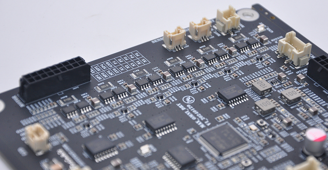
Multiple Layers
In multi-layer PCBs, the stack-up design becomes even more complex. Designers must consider how signals transition between layers, especially when vias are used, as this can affect impedance. Consistent impedance across layers requires careful planning of the stack-up, including the materials used and the thickness of each layer.
Reducing impedance in a PCB is critical, particularly in designs involving high-speed digital signals, RF circuits, or any application where maintaining signal integrity is paramount. Lowering impedance involves careful design choices and material selection.
1. Increase Trace Width
One of the most straightforward methods to reduce impedance is by increasing the width of the PCB traces. Wider traces have lower resistance because they provide a larger cross-sectional area for current to flow through. Lower resistance directly contributes to reduced impedance.
2. Optimize Stack-Up
The arrangement and spacing of layers within the PCB, known as the stack-up, significantly impact impedance. Reducing the distance between signal traces and their corresponding reference planes (ground or power planes) increases the capacitance and lowers the impedance. In multi-layer PCBs, designers can strategically place signal layers between reference planes to reduce impedance.
3. Select Appropriate Dielectric Materials
The choice of dielectric material between PCB layers has a profound impact on impedance.
Selecting materials with a low dielectric constant reduces the capacitance between traces and reference planes. Common materials like FR4 may suffice for many designs, but specialized low-Dk materials might be necessary for high-frequency or high-speed applications.
4. Minimize Trace Length
Keeping trace lengths as short as possible reduces inductive and resistive effects that contribute to higher impedance. In high-speed or high-frequency circuits, long traces can act like antennas, picking up noise and causing signal degradation.
5. Implement Proper Trace Routing Techniques
How you route traces on the PCB can also influence impedance. Sharp bends or corners in traces can cause impedance discontinuities. Rounded corners or gentle 45-degree bends are preferred to maintain consistent impedance.
6. Utilize Ground and Power Planes Effectively
Having a dedicated ground plane directly beneath signal traces creates a low-impedance path. During the PCB design, power planes should be designed to be as continuous as possible. Interruptions or splits in power planes can cause impedance variations and signal reflections.
7. Consider Controlled Impedance Simulation
Using simulation tools during the design phase can help predict the impedance of your PCB traces. Tools like Ansys HFSS, HyperLynx, or Polar Instruments' Si9000 are commonly used to model and analyze impedance in PCB designs.
Impedance control is not always necessary, but certain situations demand it:
l High-Frequency Circuits: In RF circuits, where signals operate at GHz frequencies.
l High-Speed Digital Circuits: In circuits with fast data rates, like DDR memory or high-speed serial interfaces.
l Sensitive Analog Signals: For analog circuits where signal fidelity is essential.
l Long Trace Lengths: In designs where traces are particularly long.
Knowing when to implement impedance control ensures that you don’t overcomplicate simpler designs, but still protect the integrity of complex, high-speed circuits.
Impedance control tolerance refers to how much the actual impedance can vary from the target impedance without affecting performance. Typically, this tolerance is around ±10%. However, more precise designs might require tighter tolerances, such as ±5% or even ±2%.
Meeting these tolerances requires careful design, accurate manufacturing processes, and sometimes specialized testing.
Design Stack-Up: Start by designing the stack-up, ensuring that the minimum dielectric thickness between layers is at least 50μm.
Design Circuit Width and Space Width: Use simulation calculations to design the circuit trace according to the required impedance. The trace and space widths are determined as follows for different stack-ups:
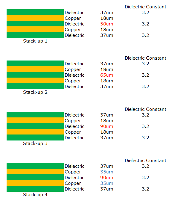
Stack-Up 1: Trace/space width is 70/130μm.
Stack-Up 2: Trace/space width is 95/140μm.
Stack-Up 3: Trace/space width is 125/130μm.
Stack-Up 4: Trace/space width is 105/150μm.
Process Parameter Control: Establish the process parameters based on the results of the first article inspection. Fine-tune these parameters to ensure consistency and precision.
Impedance Verification: During production, perform random checks on impedance to monitor and maintain quality. Additionally, conduct random checks on the finished products to ensure that the impedance meets the design specifications.
ISimply drop your email or phone number in the contact form, and we'll promptly provide you with a quotation.