EBest Circuit (Best Technology) Co.,Ltd
- +86-755-2909-1601
- sales@bestpcbs.com
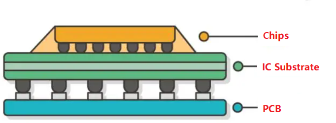
An IC substrate (or integrated circuit packaging substrate) is the base material used in the packaging of integrated circuits (ICs). Beyond protecting the bare IC, the IC substrate serves as an intermediary product connecting the chip to the circuit board. As a result, the IC substrate significantly influences circuit performance.
The IC substrate is an indispensable part of the chip packaging process. It features characteristics such as high density, precision, performance, miniaturization, and thinness. Its main function is to carry the chip. As a critical carrier in the IC packaging and testing process, the IC substrate primarily provides support, heat dissipation, and protection for the chip. It enables multi-pin connections, reduces the size of the packaging product, improves electrical performance, enhances heat dissipation, and even supports multi-chip modularity.
The IC substrate provides electrical connections between the chip and the PCB, playing a key role as an intermediary.
With the rapid development of fields such as servers, 5G, AI, and big data, the demand for high-end chips is rising, leading to rapid growth in the IC substrate industry. Additionally, IC substrates can embed passive and active components to achieve certain system functions.
Classification by Packaging Type
BGA Integrated Circuit Substrate: This is a type of IC substrate known for its excellent electrical and thermal performance. It is suitable for IC packaging with more than 300 pins because it fundamentally increases the number of chip pins.
CSP Integrated Circuit Substrate: This is a lightweight single-chip packaging type with a small-scale design. CSP IC substrates are mainly used in telecommunications and storage products with fewer pins.
FC Integrated Circuit Substrate: Flip-chip packaging offers features such as low circuit loss, low signal interference, and effective heat dissipation with strong performance.
MCM Integrated Circuit Substrate: MCM stands for Multi-Chip Module. This type of IC substrate can accommodate chips that perform various functions within a single package. This product is ideal for applications requiring thin, light, and miniaturized designs with short connections. However, it tends to perform poorly in heat dissipation, signal interference, and fine wiring due to the multiple chips being enclosed in a single package.
Classification by Material Characteristics
Rigid Integrated Circuit Substrate: Primarily composed of ABF resin, BT resin, or epoxy resin, this substrate has a coefficient of thermal expansion (CTE) of approximately 13-17ppm/°C.
Flexible Integrated Circuit Substrate: The flexible IC substrate is primarily made of PE or PI resin, with a CTE ranging from 13-27ppm/°C.
Ceramic Integrated Circuit Substrate: Containing ceramic materials such as aluminum nitride, alumina, or silicon carbide, ceramic IC substrates have a relatively low CTE, typically between 6-8ppm/°C.
Classification by Bonding Technology
l Tape-Automated Bonding (TAB)
l Wire Bonding
l Flip-Chip Bonding (FC Bonding)
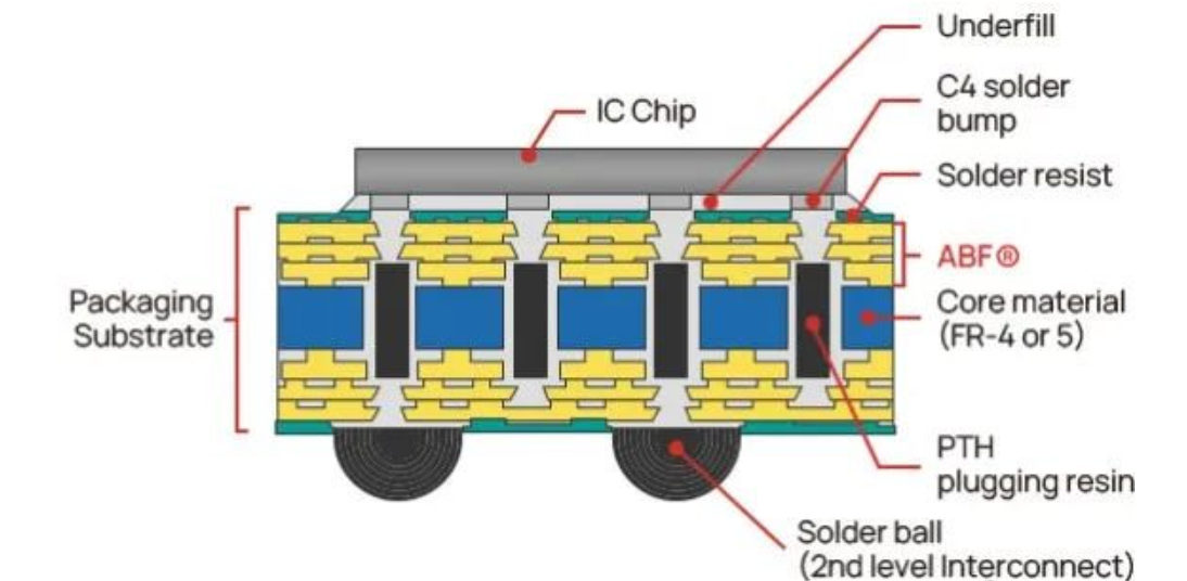
Main Raw Materials of IC Substrates: BT Substrates, ABF Substrates, and Glass Substrates
BT Substrate (Bismaleimide Triazine Resin Substrate)
The BT substrate is a type of IC substrate whose base material is BT resin, developed by Japan's Mitsubishi Gas Chemical Company. It offers advantages such as high glass transition temperature, excellent heat resistance, and low dielectric constant, making it ideal for chips that require high reliability. Its downstream applications include memory chips, MEMS chips, RF chips, and LED chips. With the rise of data processing demand driven by initiatives like "East Data, West Computing," newly built data centers are increasing the demand for server chips. Server spending accounts for roughly one-third of data center expenditures, closely linked to the capital spending of cloud computing giants. Since servers have a key storage function, they require a large number of memory chips. As domestic memory chips have achieved breakthroughs from zero to full domestic production, this has increased the demand for domestic BT substrates as supporting materials.
ABF Substrate (Ajinomoto Build-Up Film Substrate)
The ABF substrate uses ABF (Ajinomoto Build-Up Film) as its base material. This material was jointly developed by Ajinomoto and Intel, and Ajinomoto holds a monopoly on the material's production. Intel was the first to use ABF as a substrate material. The ABF substrate can achieve smaller line widths, finer circuits, and therefore, it is suitable for packaging designs with high pin counts and high transmission rates. Its downstream applications mainly include CPU, GPU, FPGA, and ASIC chips used in high-performance computing (HPC). As technology becomes more data-driven and intelligent, the precision requirements for downstream products are increasing. Combined with the rapid growth of servers and high-performance AI chips, the demand for ABF substrates continues to rise.
ABF substrates are characterized by a high number of pins, high transmission rates, precise circuitry, good conductivity, and the elimination of the need for a heat press process. They are suitable for high pin count, high transmission ICs, and are widely used in the flip-chip (FC) packaging of high-performance computing chips for 5G, AI, cloud computing, and big data analytics. In terms of packaging material costs, high-end flip-chip IC substrates account for as much as 70%-80% of the total packaging cost, making ABF substrates the most valuable material in advanced packaging processes. As computing performance continues to rapidly improve, there is a constant need for the development of ABF insulating resins with different properties. These resins must be improved to meet the demands of emerging customers’ processing technologies, along with repeated testing and validation.
As smartphones become more complex and 5G high-frequency communication transmission becomes more demanding, the thermal stability, heat dissipation, and low dielectric properties of ABF insulating materials are becoming increasingly important. However, ABF materials are currently prone to issues related to thermal expansion and contraction, leading to lower reliability. The increasing substrate area and processing complexity are expected to drive growth in the future.
Glass Substrates: A New IC Substrate Material
Glass substrates are a newly developed IC substrate material that offers excellent mechanical stability as well as superior physical and optical properties. These substrates can withstand higher temperatures and reduce pattern distortion by 50%, thereby improving the depth of focus in photolithography. They also allow for a roughly tenfold increase in via density. Additionally, the improved mechanical properties of glass lead to a much higher yield rate for ultra-large packaging.
According to Intel's analysis, glass substrates enable manufacturers to achieve performance and density gains with greater flexibility, lower overall costs, and reduced power consumption.
1. Basic definition
An IC substrate is a technology that integrates microelectronic components onto a circuit board. It is widely used in consumer electronics such as smartphones, tablets, and televisions. IC substrates require precise wiring to connect various components in an organized manner, enabling the circuit to function effectively.
A PCB is by integrating electronic components, connectors, and circuit structures onto a board. It is extensively used in fields such as computers, communication equipment, and medical devices. PCBs involve printing metal conductors on the board to connect and control electronic components.
2. Design features
IC substrates must adhere to precise dimensional standards and wiring rules to meet the requirements of miniature components. Designers face challenges such as limited circuit capacity, heat dissipation, and noise interference. IC substrate design often involves 3D modeling and detailed animation techniques to simulate and optimize circuit performance.
However, PCB design must consider factors such as materials, process costs, and manufacturing techniques, as well as the specific needs of the application. Designers must address issues like electromagnetic compatibility, circuit noise, static resistance, and noise reduction. PCB design typically involves CAD technology and circuit simulation software for optimization.
3. Manufacturing processes
IC substrate manufacturing employs advanced semiconductor processes such as deposition, exposure, etching, and molding. It requires precise laser cutting and pre-fabrication techniques. IC substrates are typically produced in batches or custom-made depending on specific requirements.
The manufacturing process of PCB includes various processes such as printing, drilling, dust removal, chemical plating, component insertion, testing, and packaging. The production requires high-precision machines and tools, including drilling machines, laser assembly machines, and static elimination devices. PCBs are typically produced in both large and small batches to meet various needs.
Despite their differences, IC substrates and PCBs share similarities in manufacturing processes, principles, and applications. Both use modular design concepts and can work together to achieve circuit functionality and optimization. The equipment and tools used in IC substrate and PCB manufacturing are also similar, such as modeling software, simulation software, and product testing instruments. Both adhere to the same circuit design principles and process standards.
l Consumer Electronics - Smartphones, laptops and tablets, wearables
l Automotive Industry - ADAS, infotainment system, EVs
l Telecommunications - 5G infrastructure, networking equipment
l Medical Devices - Implantable devices, diagnostic equipment
l Aerospace and Defense - Satellite systems, radar and surveillance system
l Industrial Applications - Robotics, automation system
l AI sensor
IC substrate packaging is typically the final stage in semiconductor device production. At this point, the semiconductor is enclosed in a protective casing that shields the integrated circuit from external damage and age-related corrosion. This packaging not only protects the semiconductor but also ensures electrical connectivity, allowing signals to be transmitted to the circuit board of an electronic device.
Here are some common types of IC substrate packages:
l Pin Grid Array (PGA) - Used for socketed components, PGA packages feature a grid of pins that connect to a socket or PCB.
l Dual Inline Package (DIP) - A traditional package where the pins extend through holes in the PCB, suitable for assemblies requiring through-hole mounting.
l Chip Scale Package (CSP) - A surface-mountable package that is significantly smaller than the die itself, often about 1.2 times the die's area.
l Quad Flat Package (QFP) - A leaded package with leads extending from all four sides. It is commonly used in surface-mount applications.
l Quad Flat No-Lead (QFN) - A compact, leadless package that closely resembles the chip size and is primarily used for surface mounting.
l Multichip Package (MCP) - Also known as multichip modules, these packages integrate multiple semi-conductor dies, discrete components, and ICs onto a single substrate, forming a larger, multifunctional IC.
l Area Array Package - This type of package optimizes space by using the entire surface area of the chip for interconnections, offering high performance and efficient use of space.
1. IC substrates are designed to accommodate a high number of interconnections between the IC and the PCB, often in multi-layered structures.
2. The materials used in IC substrates, such as low-dielectric constant materials, help minimize signal loss and maintain the integrity of high-frequency signals.
3. IC substrates ensure that signals are transmitted with minimal distortion, crucial for high-speed communication and data processing applications.
4. IC substrates are designed with materials that offer efficient heat dissipation, it is good to manage the thermal output of high-power devices like CPUs, GPUs, and power modules in electric vehicles and data centers.
5. IC substrates are built to withstand mechanical stresses, ensuring reliability in various conditions, including thermal cycling and vibration.
6. The trend towards smaller, lighter devices requires IC substrates to support compact designs with fine pitch, narrow line widths, and close spacing between components.
7. IC substrates typically feature multiple layers, allowing for more complex routing and better integration of various components such as resistors, capacitors, and inductors.
8. IC substrates are often coated or fabricated with materials that resist moisture and corrosion.
ISimply drop your email or phone number in the contact form, and we'll promptly provide you with a quotation.