Best Technology Co.,Ltd
- +86-755-2909-1601
- sales@bestpcbs.com
A High-Speed circuit board (PCB) is a circuit board specifically designed for high-speed signal transmission. High-speed signals usually refer to signals with frequencies higher than 50MHz, such as high-speed digital signals and high-speed analog signals. These signals will be affected by board materials, layout, wiring and other factors in the transmission process, so a specially designed circuit board is needed to ensure the integrity and reliability of the signal.
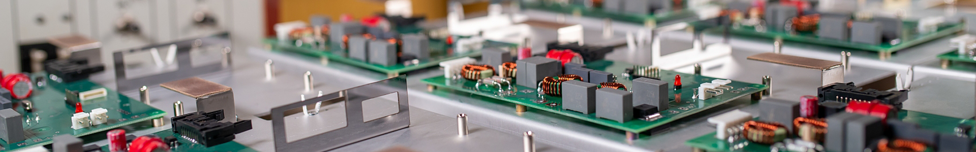
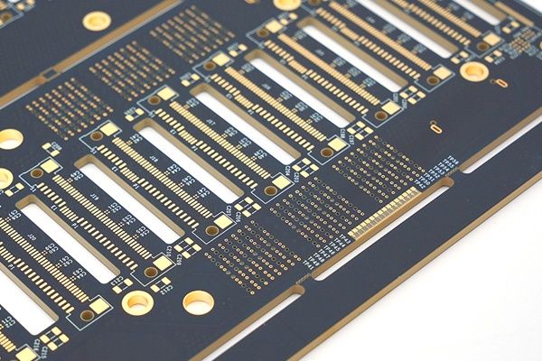
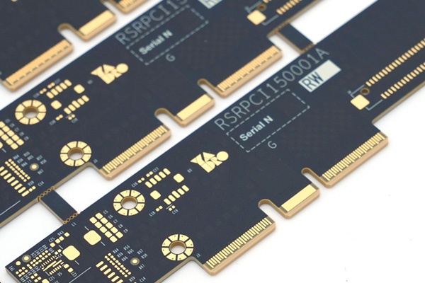
Unlike traditional PCBs, high-speed PCBs must consider signal integrity, electromagnetic interference (EMI), and proper grounding to prevent errors. These factors are particularly important in industries such as telecommunications, automotive, and aerospace, where speed and precision are critical. Here are some high speed PCB cases that we made for our customers:
The main difference between high-speed and low-speed PCBs lies in their signal frequency. Low-speed PCBs work with slower signals and don't require the same level of attention to signal integrity or EMI. In contrast, high-speed PCBs must account for the faster signals that can cause reflections, crosstalk, and noise interference.
In addition, signal transmission rate, signal rising edge and falling edge time and other parameters also affect the definition of high/low speed PCB. Specifically, it can be judged according to the following parameters:
1.Signal clock frequency: when the circuit board operating frequency is greater than 50MHz, it is generally considered to be a high-speed circuit board; When the circuit board operating frequency is less than 50MHz, it is generally considered to be a low-speed circuit board.
2. Signal transmission rate: When the signal transmission rate exceeds 1Gbps, it can be considered as a high-speed circuit board; When the signal transmission rate is less than 1Gbps, it can be considered a low-speed circuit board.
3. Signal rising edge/falling edge time: signal rising edge/falling edge time is an important factor affecting the signal transmission rate, when the signal rising edge/falling edge time is less than 500ps, it can be considered a high-speed circuit board, if it is greater than 500ps, it is considered a low-speed circuit board.
Designing a high-speed PCB is both an art and a science. It requires expertise in understanding how signals behave at high frequencies. The primary focus is on reducing noise, interference, and crosstalk, which are common issues in high-speed circuits. Prototyping is crucial to test different layouts, materials, and component placements.
Proper simulation tools help during the design phase to predict signal behavior before manufacturing. After completing the design, creating a prototype allows engineers to identify any issues with the layout, grounding, or EMI shielding, ensuring the final product performs as expected.
The choice of dielectric material is essential in high-speed applications. Dielectric materials influence how quickly signals can travel through the PCB. In high-speed designs, materials with a low dielectric constant (Dk) are preferred, as they allow for faster signal transmission.
Common materials for high-speed applications listing as below:

High-speed PCB design focuses on managing signal integrity at frequencies that can introduce noise, signal reflection, and timing issues. As the frequency increases, so does the sensitivity to these issues.
In high-speed design, the propagation delay is critical. At 60% to 70% of the speed of light, signals on a typical PCB will travel at approximately 180,000 kilometers per second. This means a signal can travel roughly 6 inches per nanosecond on an FR4-based PCB. Designers must account for this delay when timing signals, particularly in systems requiring tight synchronization.
High-speed signals require controlled impedance. Any impedance mismatches can cause reflections, leading to data loss. In designs with 50-ohm transmission lines, designers carefully calculate trace widths, the distance to the ground plane, and dielectric properties to maintain consistent impedance throughout the PCB.
Without proper termination, signals can reflect back along the transmission line. Termination resistors are used to match the impedance of the trace, effectively preventing reflections. For example, a 50-ohm resistor is used in a system designed for 50-ohm traces.
High-speed interfaces, such as USB 3.0, HDMI, and PCIe, require careful PCB design to handle fast data rates. These interfaces push the boundaries of traditional PCB design, demanding low-loss materials, precise impedance control, and short trace lengths to avoid signal degradation. Here are their functions:
Designing a high-speed PCB requires balancing several factors to ensure that signals can travel reliably across the board at high frequencies.
1. Signal Integrity
Ensuring signal integrity involves maintaining consistent impedance, reducing signal noise, and preventing reflections. When frequencies rise above 1 GHz, where timing mismatches and impedance deviations can lead to data loss.
2. Electromagnetic Interference (EMI)
High-speed circuits emit more electromagnetic energy, increasing the risk of EMI. Shielding and grounding play a critical role in managing EMI. Placing high-speed signals on internal layers surrounded by ground planes reduces external interference. Designers aim for shielding effectiveness greater than 20 dB in most high-speed applications.
3. Thermal Management
High-speed circuits generate more heat, especially in complex designs. In some high-speed boards, thermal dissipation techniques such as heat sinks and thermal vias are used to manage temperatures that could reach 85°C or higher. Proper thermal management ensures that components operate within their safe temperature range.
4. Power Distribution
Stable power distribution is critical in high-speed designs. Designers use power planes and decoupling capacitors to ensure a consistent supply of power. Voltage drops or noise in the power supply can lead to performance degradation, especially in systems requiring low noise levels below 5 mV.
5. Material Selection
The material used in high-speed PCBs impacts performance. For instance, FR4 has a Dk of 4.5, making it suitable for frequencies up to 1 GHz. For higher frequencies, materials like Rogers 4000 or PTFE (Dk of 2.0 to 2.5) are preferred, as they provide lower signal loss and better signal integrity at high frequencies.
6. Component Placement
The placement of components on high-speed PCBs is critical to signal integrity. Key components like processors and memory modules are placed as close as possible to reduce trace lengths and minimize signal delay. For instance, placing high-speed chips within 10 millimeters of each other can significantly improve performance.
The manufacturing process of high-speed PCBs is more intricate than that of standard PCBs due to the critical need to maintain signal integrity and prevent issues like signal distortion, electromagnetic interference (EMI), and crosstalk at high frequencies.
1. Material Selection
Material selection is one of the most critical steps in the manufacturing process of high-speed PCBs. Standard FR4 PCB material with a Dk of around 4.5, suitable for frequencies up to 1 GHz. Rogers (RO4000/RO3000 series) are High-performance materials with lower Dk values (2.0 to 3.5), designed for frequencies above 1 GHz, commonly used in RF applications. PTFE offers excellent electrical properties with a Dk of around 2.0, commonly used in PCBs for 5G, automotive radar, and microwave applications.
2. Layer Stack-Up Design
In this step, PCB manufacturers determine the number and arrangement of layers, including signal layers, power/ground planes, and insulation layers. Signal layers are paired with ground planes to minimize EMI and crosstalk. For high-speed designs, the layer stack-up is carefully calculated to control impedance (usually 50 ohms or 90 ohms for differential pairs).
3. Trace Width Calculation and Impedance Control
In high-speed PCB manufacturing, accurate trace width and spacing are crucial to achieving controlled impedance. For example, a 50-ohm trace is typical for single-ended signals, while 90-ohm differential pairs are used for high-speed interfaces like USB, PCIe, and HDMI. You can use some advanced software tools like Best Technology trace width calculator.
4. Lamination
Once the materials and stack-up are prepared, the lamination process begins. The layers are pressed together under high pressure and temperature in a vacuum to remove any air pockets.
5. Drilling and Via Formation
High-speed PCBs often feature a combination of through-hole vias, blind vias, and buried vias. Via placement and size are carefully calculated to avoid introducing signal delays or reflections. Laser drilling is often used for microvias (small vias) in HDI PCBs, which are common in high-speed designs. Microvias reduce parasitic capacitance and inductance, ensuring faster signal transitions.
6. Copper Plating
After the vias and holes are drilled, the next step is the copper plating process. A thin layer of copper is applied to the entire board, including the hole walls, to create electrical connections between layers.
7. Etching
In this step, the excess copper is removed to define the traces and pads on the PCB. For high-speed PCBs, the etching process must be extremely precise to avoid variations in trace width, which can affect signal integrity. Any over-etching or under-etching can result in impedance mismatches, causing signal reflections.
8. Solder Mask and Silkscreen
The solder mask is applied to the PCB to protect the copper traces and prevent short circuits during component assembly. Once the solder mask is applied, the silkscreen (labeling) is printed on the board to provide identifiers for components.
9. Surface Finish
The surface finish provides a protective coating on the exposed copper areas, ensuring good solderability and preventing oxidation. Common finishes for high-speed PCBs include: ENIG - OSP - Immersion Silver
10. Testing and Inspection
The final stage involves thorough testing and inspection to ensure the high-speed PCB meets design specifications and performance requirements.
High-speed PCBs are used in a wide range of industries, including:
As technology advances, the demand for high-speed PCBs will only continue to grow.
ISimply drop your email or phone number in the contact form, and we'll promptly provide you with a quotation.