Best Technology Co.,Ltd
- +86-755-2909-1601
- sales@bestpcbs.com
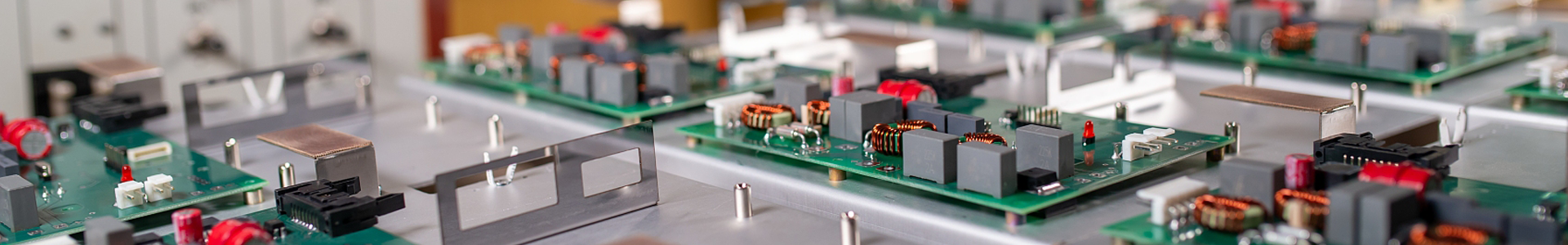
A single-sided PCB, also known as 1 layer PCB. As the name suggests, is a printed circuit board (PCB) that has its components and circuitry on just one side of the board. These boards are among the most basic types of PCBs available. They consist of a single layer of conductive material, typically copper, applied to one side of a non-conductive substrate like fiberglass or FR4 material. The components are placed on the copper side, and the electrical connections between these components are made by etched pathways on the same side.
Single-sided PCBs are widely used in simple electronic devices where the complexity of the circuit does not require multiple layers. Due to their simplicity, single sided PCBs are widely used in products like calculators, power supplies, and LED lighting systems.
The manufacturing process of single sided PCBs is straightforward and involves several key steps:

Here's a step-by-step look at how these PCBs are typically produced:
Design and Layout: The first step involves designing the circuit layout. Engineers use CAD software to create a blueprint of the PCB, including the placement of components and the routing of electrical connections.
Substrate Preparation: The substrate, usually made of fiberglass, is cut to the desired size. This substrate provides the base onto which the copper layer will be applied.
Copper Lamination: A thin layer of copper is laminated onto one side of the substrate. This copper layer will eventually be etched away to form the circuit pathways.
Photoresist Apply: A photoresist, which is a light-sensitive material, is applied over the copper layer. This photoresist will protect the areas of the copper that need to remain during the etching process.
Exposure and Development: The board is exposed to ultraviolet (UV) light through a mask that covers the areas of the photoresist that should not be hardened. After exposure, the board is developed, and the unhardened photoresist is washed away, revealing the copper underneath.
Etching: The board is then subjected to a chemical etching process. The etching solution removes the exposed copper, leaving only the copper that was protected by the hardened photoresist. This forms the conductive pathways on the PCB.
Solder Mask Apply: A solder mask, typically green, is applied over the entire board. The solder mask helps prevent solder bridges from forming during the soldering process and protects the copper traces from corrosion.
Component Placement and Soldering: The electronic components are placed on the board in their designated positions, this is the SMT assembly process. And soldering is performed to secure them in place and establish electrical connections.
Testing and Quality Control: The finished PCB undergoes testing to ensure that all connections are correct and that the board functions as intended. Any defects are identified and corrected during this stage.
Single sided PCBs offer several advantages that make them a preferred choice for many applications:
l Cost-effectiveness
l Ease to design
l Quick turnaround time
l Fast delivery
l Ease of maintenance
l Quick manufacturing
l Reliability
l Ideal for simple circuits
l Environmental friendliness
l Widely usage
A double sided PCB is a step up from single sided PCBs in terms of complexity and functionality. Unlike single sided PCBs, double sided PCBs have conductive layers on both sides of the substrate. This allows for more complex circuit designs, as components can be mounted on both sides of the board, and conductive traces can connect components on either side through plated through-holes.
In a double-sided PCB, vias (small holes) are used to connect traces from one side of the board to the other double sided PCBs are commonly used in more sophisticated electronics where space constraints and circuit complexity require more than a single layer. Examples include automotive electronics, communication devices, and industrial control systems.
The key difference between single and double sided PCBs lies in their ability to handle more complex circuits. Double sided PCBs offer greater flexibility and are better suited for applications that require higher performance and more connections.
While single-sided and double-sided PCBs are relatively simple in design, multilayer PCBs are much more complex. Multilayer PCBs consist of multiple layers of conductive material, separated by insulating layers, all laminated together. These boards can have three or more layers, depending on the design requirements. The key differences between single and multilayer PCBs are:
1. Complexity
The complexity including manufacturing and circuits. Multilayer PCBs can handle much more complex circuits due to the increased number of layers. They allow for higher component density and more advanced functionality. And meanwhile, it has much complex manufacturing process when comparing single sided PCB.
2. Circuit density
Multilayer circuit boards can achieve more complex wiring in a limited space, so the wiring density is higher and more electronic components can be accommodated.
3. Performance
Multilayer circuit boards with more conductive layers can provide better signal integrity and electromagnetic compatibility, thereby improving the performance and reliability of the circuit.
4. Size
Multilayer PCBs can achieve the same functionality as a single-sided PCB in a much smaller footprint.
5. Cost
The manufacturing process for multilayer PCBs is more intricate and involves more materials, so they are more expensive to produce than single-sided PCBs. The more layers of PCB, the cost will much higher.
6. Applications
Single-layer circuit boards are usually used in simple electronic devices, such as toys, calculators, etc. The multi-layer circuit board is widely used in computer, communication equipment, automotive electronics and other high-performance electronic equipment.
The thickness of a single sided PCB can vary depending on the application and manufacturer specifications. a typical single sided circuit board is usually between 0.6mm and 1.6mm, of which 0.6mm, 0.8mm, 1.0mm, 1.2mm, 1.6mm are more common. This thickness includes the substrate, the copper layer, and any additional protective layers like the solder mask.
The choice of thickness is influenced by factors such as mechanical strength, space constraints, and the intended use of the PCB. For instance, thicker PCBs may be used in applications requiring greater durability or where mechanical stress is a concern. In general, under normal circumstances, the use of 0.8-1.0mm thickness can meet most of the needs.
At Best Technology, we understand the importance of selecting the right PCB thickness for your project. Our team can help you choose the optimal thickness to ensure your PCB meets all necessary performance and durability requirements.
At Best Technology, we specialize in producing high-quality PCBs tailored to your specific needs. With 18+ years of experience in the PCB industry, we pride ourselves on delivering reliable, cost-effective solutions for our clients. Our state-of-the-art manufacturing facilities ensure that each PCB meets the highest standards of quality and performance.
Whether you need a simple single sided PCB or a more complex multilayer design, Best Technology is here to help. Our team of experts is dedicated to providing exceptional customer service. Contact us today to learn more about our services and how we can assist with your PCB needs.
ISimply drop your email or phone number in the contact form, and we'll promptly provide you with a quotation.