T:+86-755 2909-1601/1602/1603
Phone +86-18923412995
Email Us: sales@bestpcbs.com

In fact, the process of laser drilling/scribing and stencil making can be done at the same time, as they’re belonging to different production workshop.
(1)Stencil: Hard aluminum or aluminum alloy is commonly be used in the stencil of the thick film circuit. The size of the stencil is generally 100 mm×150 mm or 150 mm×200 mm, and rectangular is the normal outline.
(2) Foil: The foil of the thick film circuit is generally used stainless steel or nylon.  
(3)Photosensitive glue: As the trace of the thick film circuit requires a thick ink film, it is necessary to use Photosensitive glue which can coating the optical film from 20~30μm and have no edge defects after development.

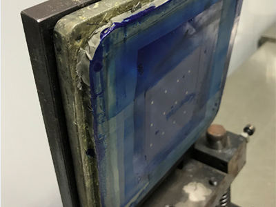
The picture below is the front side of the stencil (It has been already installed on the manual printing table)
the-front-side-of-the-stencil.png the-front-side-of-the-stencil-2.png

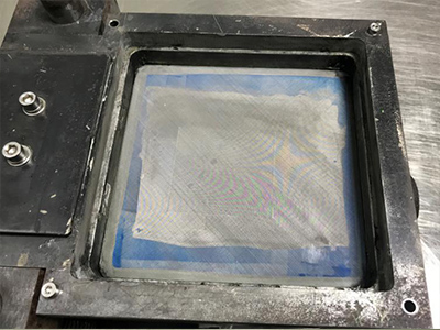
The stencil is installed on the printer working table and is ready for printing.

the-stencil-is-installed-on-the-printer-working-table

The size and the outline of the stencil will be different if it is used on the automatic or semi-automatic printing machine,.
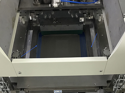
stencil-on-the-printing-machine

The rectangular stencil is used to print the cylindrical substrate.
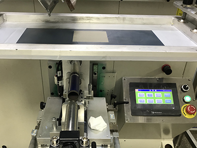
print-the-cylindrical-substrate

Now let’s move to the next step Conductive ink preparation . If you have any questions about the last step, please back to the Blackening spot removing after laser drilling