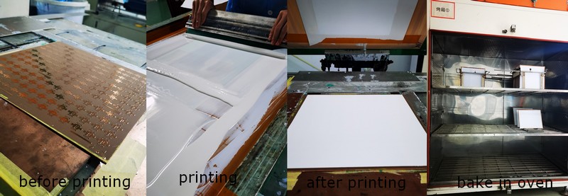
Similar like FR4 PCB, soldermask and silkscreen making is the same like other normal PCB. Here are some simple basic process showing soldermask making of SinkaPAD board (SinkPAD PCB).
After hot lamination process, SinkPAD board need to be cleaned again and then go to next step of solder mask making.
Firstly, using correct stencil and align SinkPAD PCB with stencil;
Secondly, print the oil (solder mask) (normal color is white and black, green, blue, yellow, red color available too), via handle (samples & small order) or auto-printer (big volume production), on surface of SinkPAD board;
Thirdly, after 1 hours standing by, the boards will be sent to oven for baking;
 (Soldermask printing & baking)
Fourthly, using soldermask film, to develop the soldermask using UV light or other type of lighting, to exposure the soldermask;
Fifthly: Etching the board and finally the soldermask will come out.
 (soldermask develoing & etching process)
Normally the surface finishing of SinkPAD board are OSP, ENIG. And there’s no HAL(LF) as the process is not good enough for Sink PAD PCB. Other special finishing are available upon request.
Each process will be monitored to make sure beautiful soldermask, silkscreen, surface finishing will be made according to customers’ drawings. Please contact us if you want to know more about that series of manufacturing process.
After soldermask, silkscreen will be printed, before or after surface finishing which normally is ENIG, OSP.
Return to main manufacturing process
Or go to next step of Outline & Testing process.